PIC12F683 High Voltage Flyback Transformer Driver

PIC12F683 High Voltage Flyback Transformer DriverA friend at Purdue University (Sumanth Peddamatham) helped motivate and inspire me to create a high voltage flyback transformer driver for a computer CRT flyback transformer. While the schematic and code for driving the transformer are extremely straightforward and simple, finding and obtaining a high quality solid state flyback transformer can be difficult. Please note that the voltages generated by the flyback transformer are potentially very dangerous, so extreme care must be exercised when building and/or using the schematic presented in this project. Diode split flyback transformers (like the one used in this project) can output 25kV or more.

Disclaimer: The high voltage devices and schematics presented on this website (https://www.semifluid.com) and the pages herein are for educational and experimental purposes only. Build and/or use at your own risk. I cannot be held liable or responsible and will not accept any type of liability in any event, in case of injury, damage to persons or property, or even death by building and/or using this device or any other high voltage device posted on this website. By accessing, reading, and/or printing the articles presented here you agree to be solely responsible and exempt me from any criminal and/or lability charges and/or suits. Please note that safety is the primary concern when working with high voltage circuits. Always be careful, use extreme caution with high voltage circuits, and play it safe!

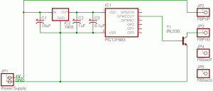
Here is the full schematic for the driver. Yes, it is this simple. All that is needed is a power supply (preferably >9V), a 7805 +5V linear voltage regulator, decoupling capacitors (C1, C2, & C3), a PIC12F683, a suitable logic level power MOSFET (I used an IRL530), and a flyback transformer. It is important to note that the MOSFET needs to be heatsinked, otherwise it could overheat.

JP2 (FBPriP) is the positive input of the primary winding, JP3 (FBPriG) is the ground/negative input of the primary winding, and JP4 (FBSecP) and JP5 (FBSecG) are the positive and negative outputs of the secondary winding where the high voltage is generated.

The flyback transformer was found in a broken 21″ CRT monitor. An alternative to opening a CRT and exposing yourself to potentially harmful voltages is to purchase a replacement flyback transformer from a surplus store or from eBay. I experimented with the driving frequency to find the optimal output and found that 20kHz produced the longest arcs for this flyback transformer.

As always, please feel free to contact me if you have any questions about the setup and as the disclaimer above says: Always be careful, use extreme caution with high voltage circuits, and play it safe!

Source Code
This is the source code for the driver. Please note that the driving frequency can be adjusted by changing the following line:

delay_us(25);

12F683 Flyback Driver.c (hex)

Videos
Here are three videos of the PIC12F683 High Voltage Flyback Transformer Driver in action. The first video demonstrates the high voltage arcing through a beercap-ful of beer (Stella Artois) with a power supply voltage of 9V. The second video demonstrates the high voltage arcing through a cap-ful of rum (Sailor Jerry) with a 24V supply voltage. The third video demonstrates the high voltage arcing through a cap-ful of pancake syrup with a 24V supply voltage.

Pictures
Here are a couple of pictures from experimenting with the driver:
High Voltage Over and Through Red LED
High Voltage Sparks

25 thoughts to “PIC12F683 High Voltage Flyback Transformer Driver”

  1. Hi,

    Your idea is very interesting and I will build such a generator once I get a HV transformer!
    However, I think that you should add a so-called “freewheel” diod across the transformers’primary to protect the power MOSFET against high voltage spikes occuring when the transistor blocks.
    Use a fast-recovery, several-amps-forward-current-diod, you can find such a diod in a roasted switching power supply for example.

    Regards,

    Olivier
    PhD student,
    LIRMM, Montpellier, France
    http://www.lirmm.fr

  2. Just a note to Olivier – If you check the data sheet for the the IRL530 you will note that it has a suppression diode built in, as do many “power” FET’s

  3. Hello Doug (from comment n°4)

    Datasheets give you some data about the device, but it’s far from being a complete description of it. Here is an interesting “Power MOSFET basics”, from the manufacturer of the IRL530, International Rectifier:
    http://www.irf.com/technical-info/appnotes/mosfet.pdf
    The “protection diod”, or more precisely “body diod” seen in the datasheet simply comes from the structure of the power MOSFET. In our case, where we switch a coil, that is, an inductive load, this “body diod” is useless, since the inductive overshoot appearing while you turn off the MOS will tie the drain up to dramatically high voltages, exceeding the drain-to-source breakdown voltage specified in the datasheet (only 100V), thus leading to a short lifetime of the MOSFET. Consequently, I think that a protection diod would be more effective in parallel to the coil instead of the MOSFET channel. You often see such protection diodes mounted across relay coils, for example.

    Regards,

    Olivier
    PhD student,
    LIRMM, Montpellier, France
    http://www.lirmm.fr

  4. To Oliver : These protection diodes are not to be use! Flyback transformers use the inductive kick to boost up primary voltage, and then the kick is amplified by turn ratio. By adding a clipping diode you will weaken the voltage of the secondary.

    To page writer : Sorry but you’re using a pretty weird circuit to drive your flyback. Why use PIC? A simple astable 555 would be just right because you could power the IC with a higher voltage (and so drive the mosfet with higher voltage). Also, use better mosfet, 100 V is way to low. you need at least 200 V, 600 V would be better, so you could have BIG kickbacks. Also use higher primary voltage (60 V is great). All of this is to boost at maximum the primary voltage by using the maximum shutdown speed of the mosfet.

  5. Sorry, that’s right, the protection diode in parallel with the primary would simply annihilate the inductive energy. But anyway, in the flyback converter, inductive energy has to be collected by the secondary when the power transistor blocks at the primary. In our case, the secondary collects energy by sparking, but as long as there’s no spark, then the primary undergoes a potentially high inductive kick. A MOS with high breakdown may not be enough, a transient suppressor might be helpfull in parallel to the primary coil (transil diod, …)
    Playing with unclamped inductive overshoots is somewhat like playing with fire 😉
    Another idea: put a capacitance in parallel to the secondary coil to make a resonant LC circuit. Driven by the primary nearly it’s resonant frequency, it would produce a great overvoltage. Of course it requires a high voltage cap… and great care.
    Tesla coils are also cool stuff.

    Olivier

  6. The ideal flyback driver will use a current-limited control IC.
    Several issues are important to efficiency and safety (to the circuit).

    1. if you drive the core into saturation, it will blow up the mosfet. Since saturation flux is more or less fixed (about 0.3 tesla for ferrite materials), the current you can drive through the core is determined by the air gap in the core and number of turns in the primary. Current in the primary is determined by switch on-time and power supply voltage.

    The point is, the on-time of the switch should vary with the input voltage. The easy way to do this is just to have a boost-converter controller IC with built-in mosfet gate driver, which measures the current across a small sense resistor under the source of the mosfet. If you don’t want to do that, then use the PIC with some kind of a peak-holder circuit to measure the peak current. You will see as you increase the duty-cycle of the FET that the current increases linearly at first, then starts upwards on an exponential climb. This is the stairway to FET heaven! Don’t let the duty cycle go beyond the linear region of the core, for good efficiency and healthy FET lifetimes.

    2. You need a gate driver for the mosfet. A PIC is not strong enough to switch it on and off fast enough for good efficiency. Ideally there should be above an amp of instantaneous current. Most fets have more than 1000 pF of gate capacitance. Particularly when switching large drain voltages, the “miller effect” makes the apparent capacitance at the gate much larger. In a flyback, on turnoff the leakage inductance of the transformer creates a very large spike, which makes gate turnoff slow. Don’t neglect this!

    3. use a high-voltage fet. as mentioned before, 600 V would be excellent. The higher the clamping voltage, the less efficiency lost!

    4. generally, a high-power flyback driver will not clamp the transient by using the FET in avalanche mode. I think this is for reasons of speed. Generally, a zener diode clamp is used a lower powers, and at higher voltages (where it is hard to find zener diodes), a “freewheeling diode” in series with a parallel R/C filter is used.
    There are also power transistor-based “zener boosters” that can be used. (details on request 😉

    5. because the copper losses are proportional to I^2 * R, the delicate secondary windings are probably the limiting factor for your power output. This implies the flyback should be driven in “continuous conduction mode”, rather than “discontinuous conduction mode”–this reduces the ripple current through the windings and diodes, and ought to maximize output power the windings can handle.

    6. best efficiency is said to be achieved when core and winding losses are equal. To my thoughts, this implies increasing the switching frequency until core losses become significant.

    7. output regulation! It is very difficult to directly regulate the high-voltage output. Perhaps for current-sensing the output you could make a floating optocoupler in opaque plastic tubing using an LED’s pretty linear current-to-light output, driving a photocell. For measuring voltage, either a voltage divider made from PVC pipe filled with a calculated concentration of copper sulfate solution (this allows very high resistances to be made), or else sense the reflected voltage from a low-voltage winding. Subject to the limits of transformer coupling, the voltage wave obtained from another coil on the transformer will tell you what voltage is “seen” by the secondary coil. If you regulate this voltage, it will also regulate the secondary. This is called “cross-regulation”. It’s not perfect, but a whole lot better than nothing at all. One limitation to this method is that without any load, regulation will suck. For a high-voltage output, I will guess that corona losses will load it enough that this is not a problem.

    With a PIC in there, you can have cool stuff like digital HV output meter (voltage, current, and power), and with a high enough switching frequency, the possibility of making controlled output waveforms.

    Good luck….

  7. hi, good workman, nice project.
    i have a project that gives a variable output high voltage
    e.g from 0 till 25kv.
    what you did, is great, but if i change the frequency that
    drives the mosfet, could that gives variable high voltage on
    the secondary flyback?
    thanks .

  8. Pingback: This High Voltage Flyback Transformer Driver is Remarkable! - CircuitGeek
  9. best greetings

    dear sir
    thank you for your best site , it’s give me much pleasure to benefit of your experiments and

    development My ideas.

    dear sir ,can you assistance me about ; how to transformer to high volts of flyback to simple

    volts ; please any assistance contact me soon

    mora_1236@hotmail.com mY name : aziz from Morocco age 32 years
    thank you with best wishes

  10. Well, you can use a small Radio-frequency tunable transformer to pump up the Gate drive voltage, however, you can use MOSFET driver if you want to.

    Regarding to the MOSFET voltage, the Japanese MOSFET (Mitsubishi or Toshiba) is the way to go, since these are the most common brand used by power supply in TV and monitor, regarding the low chance of failure. Just use the largest of all if you can (TO-220AB or 227)

  11. Hey, great job.
    I need a little help here. I have e17865 and I’m really confused which pin is “FBPriP”, “FBPriG” and so I have no idea where to connect the microcontroller.
    Can you help me? Thanks.

  12. FBPri = Flyback primary winding (thin pins on the bottom of the flyback, you must find it out wich pair to use)

    FBSec = Flyback secondary winding (one thick wire that comes out on the top of the flyback, and the other, the ground, is a pin located on the bottom of the flyback, you must find this too)

    to find the pairs that match, use a voltimeter, you should read a very low resistance for the primary, i think that should have less than 5 ohms, becouse the primary has less than 100 turns of wire, it works with 150v, and more than 20 ohm for the secondary, becouse has more than 1000 turns of wire, the relation between primary and secondary is how much the flyback will amplify the voltage, i don’t have a flyback right here to test it. there are special pins on the bottom for different propouses, this give us different voltages too, but not as much as 10kv. some flybacks has a voltage doubler / triplier to elevate even more the voltage up to 25kv / 30kv, also if you wish to increase even more the voltage you can use the marx generator at the output of the secondary… it’s very interesting.

    i’m sorry if my english is not clear enough, i’m out of practice…

    regards from argentina!!!

    PD: steven, very good ideas, i’m learning a lot reading all your projects, i’m making the osciloscope and other stuff too…

  13. Hi
    most mains-operated CRT-TVs used bipolar transistors for H-output stage, with Vcs ratings of 1100-1500V. I suggest take a good hard look at Service Manuals and any other supporting literature of large TVs, with particular attention to the base-drive arrangements because it is crucial to survival of these devices.
    The many auxiliary windings are variously used to drive dynamic-convergence, East-West modulator/vertical output stage, etc. Partly for cost reasons but also in absence of perfect regulation o fEHT, the deflection-circuits need to DECREASE their output as EHT load increases with brightness – this maintains picture at correct size (more or less!) as picture-content and user-set brightness varies.
    TV scanning uses roughly 52 us scan (“ON”) time and 12us flyback (“OFF”) – this is probably the best way to run these LOPTs.

  14. I had good success with this after changing PIN_A1 to PIN_A4 in the code. Initially I made a mistake in my PCB layout based on the schematic for pin 3 signal out. PIN_A4 corresponds to the pin shown in the schematic.

    I see super good efficiency running .6 amps from 15v across the primary with a 5/8″ arc. I’m very impressed by how well this works with a N channel irf840 mosfet, sony color tv flyback xformer and delay_us (28) ;

    Great design.

Leave a Reply to MCancel reply

This site uses Akismet to reduce spam. Learn how your comment data is processed.